Powering Change
Installing since 2010 · 0118 951 4490 · info@spiritenergy.co.uk


To see how solar works, let's look at a typical PV system:
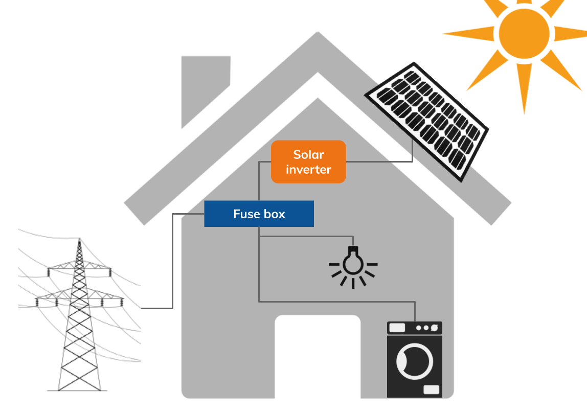
Grid-connected photovoltaic systems are the most common type as they make use of the existing mains electricity grid. They are simpler in design and easier to fit than off-grid systems. The electricity produced during the daytime is either used by the property owner, or directed back into the electricity grid and purchased by a utility company, an arrangement called ‘net metering’. At night, or on dark days when the panels do not produce sufficient power, electricity will be supplied via normal utility company grid system.
Domestic battery storage has taken off in the last few years - we're now installing it alongside many PV systems. These batteries allow you to store energy you generate on site, rather than send to the grid, for use later when needed.
Far less common is an 'off-grid' or 'stand alone' system, which produces and stores power independently from the utility grid. These systems are particularly suitable in remote locations especially those where the property is more than one-quarter mile from the nearest power lines. Often the installation of an off-grid PV system proves more cost effective than extending the power lines. The electricity generated by the panels is stored in a bank of rechargeable DC batteries (and may also be diverted into the hot water tank or heating system). In order to power household appliances an inverter will be required to convert the stored DC to AC. A generator is usually also required to achieve a cost effective and continuous electricity supply.
To really understand how PV works, we need to dig deeper into the panel components. Here’s a quick explanation of how a silicon solar cell works.
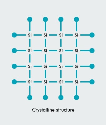
An atom of silicon has 14 electrons, arranged in three different shells. The inner shell has two electrons and the next shell has eight. Both are full. However the outer shell is only half full with just four electrons, and thus the atom is always looking for four more electrons to fill up its outer shell. It does this by covalent bonding i.e sharing electrons with four nearby atoms (one per atom). This forms a crystalline structure, as in this diagram:
Pure crystalline silicon is a poor conductor of electricity because none of its electrons are free to move about. However to make a solar cell, other atoms ('impurities') are deliberately added, primarily phosphorous (which has five electrons in its outer shell) and boron (three electrons in its outer shell), to the silicon atoms.
Consider the crystalline silicon lattice above with an atom of phosphorous (5 electrons in its outer shell) substituted for an atom of silicon here and there. The phosphorous will still bond with the neighbouring silicon atoms, but there will be one electron left over that doesn't form part of a bond. Light energy (photons) can easily knock this spare electron loose.
The process of adding impurities on purpose is called doping, and when doped with phosphorous, the resulting silicon is called N-type ('n' for negative) because of the prevalence of free electrons. N-type doped silicon is a much better electrical conductor than pure silicon.
As well as a layer of N-type silicon, a solar cell also needs a layer of 'P-type' silicon. This is silicon doped with the element boron, which has only three electrons in its outer shell instead of four. Instead of having free electrons, P-type ('p' for positive) has free openings and carries the opposite (positive) charge. These openings are known as 'holes'.
When the N-type and P-type silicon come into contact an electric field is created. At the junction, an 'equilibrium' is reached whereby electrons trying to cross from the 'N' side to the 'P' side are prevented from doing so by something called the PN Junction.
When newly doped N-type and P-type semiconductor materials ('wafers') are fused together, they create what is known as a 'PN Junction'.
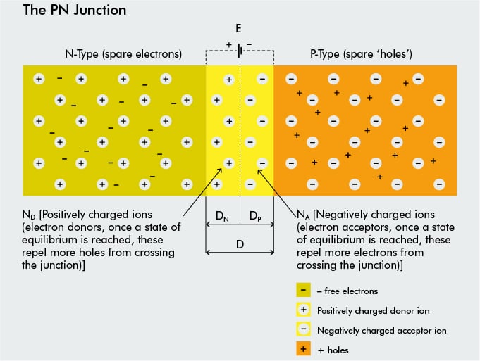
When they are first joined together a very large density gradient exists between both sides of the PN junction. The result is that some of the free electrons from the phosphorous impurity atoms on the N side begin to migrate across this newly formed junction to fill up the holes on the P side, thus producing negative ions (NA) on the P side, and leaving behind positively charged donor ions on the N side (ND).
Now the holes from the P side migrate across the junction in the opposite direction into the region where there are large numbers of free electrons. As a result, the charge density of the P-type material along the junction becomes negative as it is left with negatively charged acceptor ions (NA). Similarly, the charge density of the N-type material along the junction becomes positive. This charge transfer of electrons and holes across the PN junction is known as diffusion.
This process continues back and forth until the number of electrons which have crossed the junction have a large enough electrical charge to repel or prevent any more charge carriers from crossing over the junction. Eventually a state of equilibrium occurs producing a 'potential barrier zone' around the area of the junction as the donor atoms (ND) repel the holes and the acceptor atoms (NA) repel the electrons.
The width of these P and N layers depends on how heavily each side is doped with acceptor density NA, and donor density ND, respectively.
Since no free charge carriers can rest in a position where there is a potential barrier, the regions on either sides of the junction now become completely depleted of free carriers in comparison to the N and P type materials further away from the junction. This area around the PN Junction is now called the Depletion Layer.
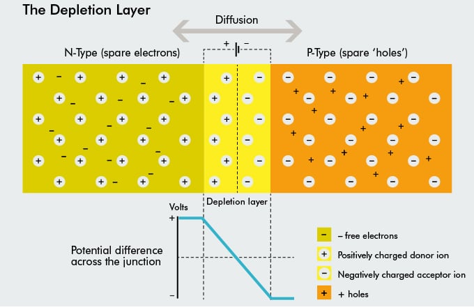
The total charge on each side of a PN Junction must be equal and opposite to maintain a neutral charge condition around the junction. If the depletion layer region has a distance D, it therefore must therefore penetrate into the silicon by a distance of Dp for the positive side, and a distance of Dn for the negative side giving a relationship between the two of: Dp*NA = Dn*ND (NA / ND being charge densities) in order to maintain charge neutrality (equilibrium).
Overall, the N-type material has lost electrons and the P-type has lost holes, so the N-type material has become positive with respect to the P-type and the N-side is at a positive voltage relative to the P-side. A free charge can only cross the depletion region if it is given extra energy by an external source.
When light (photons) hits the solar cell, its energy breaks apart electron-hole pairs. Each photon with enough energy will normally free exactly one electron, resulting in a free hole as well. The field will send the electron to the N side and the hole to the P side. This disrupts the electrical equilibrium, and if an external current path is provided, electrons will flow through the path to the P side to unite with holes that the electric field sent there. The electron flow provides the current, and the cell's electric field causes a voltage.
Note that at room temperature the voltage across the depletion layer for silicon is about 0.6 volts.
To summarise, as per the previous section, a solar cell consists of two thin layers of semi-conductor (usually silicon), that have been doped with specific chemicals (boron, phosphorous).
Sunlight shining on the solar cell knocks electrons from the orbits of the doped semi-conductor in sufficient numbers to generate a direct current (DC).
The cell is covered with a thin layer of anti-reflective coating (ARC) to minimise light reflection. Silicon is a shiny material which would otherwise reflect the light before it had done its job.
The top semi-conducting layer, or ‘N’ type layer, is doped with tiny amounts of phosphorus so that almost every thousandth silicon atom is replaced by a phosphorus atom. This creates free moving negative charges called ‘electrons’.
The base semi-conducting layer, or ‘P’ type layer, is doped with minuscule amounts of boron so that almost every millionth silicon atom is replaced by a boron atom. This creates free moving positive charges called ‘holes’.
When the ‘N’ and ‘P’ type layers are placed close together, as they are in a solar cell, the positively charged ‘holes’ and the negatively charged ‘electrons’ are attracted to each other. As they move into their respective neighbouring layers they cross a boundary layer called the ‘PN Junction’. This movement of negatively and positively charged particles generates a strong electrical field across the PN Junction. When sunlight strikes this field it causes the electron particles and the hole particles to separate, which in turn creates a voltage of around 0.6V.
The voltage pushes the flow of electrons or ‘DC current’ to contacts at the front and back of the cell where it is conducted away along the wiring circuitry that connects the cells together.
The basic structure of a solar cell is shown in the diagram below.
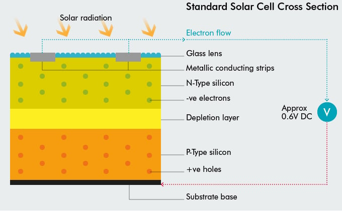
From top to bottom:
As an individual solar cell only generates a low voltage, approx 0.5V - 0.6V. A number of cells are wired together to form a solar panel or ‘module’ that can generate anything between 80–360 watts. Typically 60 cells or 72 cells are combined into a single module.
Solar panels are strung together in an array, which forms your solar system.
To find out more about how PV systems work for your home, download our expert guide: